+86-13925515590
 kleinma@aliyun.com

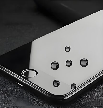
Custom Electronic Glass for Displays & Electronic Devices
Electronic Glass for Electronic Devices
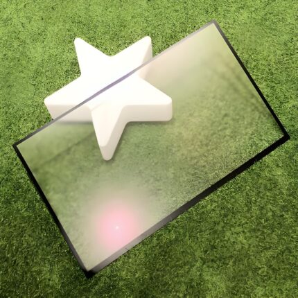
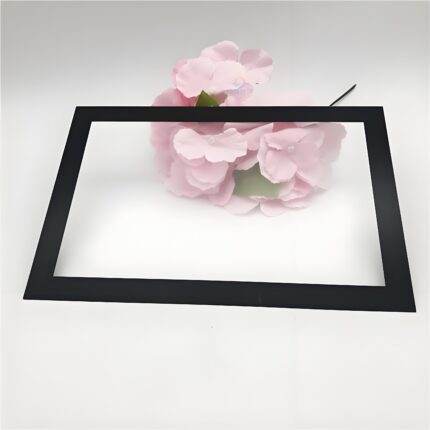
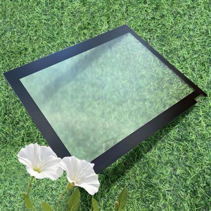
Electronic cover glass is a precision glass component used in displays, touchscreens, control panels, consumer electronics and other electronic devices. As a professional electronic cover glass manufacturer, Weiman provides custom glass solutions based on your required material, thickness, dimensions, shape, optical performance and surface treatment.
Our electronic cover glass can be processed through precision cutting, CNC machining, edge processing, chemical strengthening, thermal tempering, screen printing, AR/AG/AF coatings, adhesive bonding and OCA lamination. These processes allow us to produce electronic cover glass components that match different display and device designs.
We support OEM and custom electronic cover glass projects from drawings or samples to mass production. Whether you need thin display glass, touchscreen cover glass, printed glass panels or customized glass components, our engineering team can evaluate your specifications and recommend a suitable glass material and processing solution.
In Weiman, we offer premium glass OEM service including:
Cutting: Rough shapes by diamond unit or laser cutting from big sheet of electronic glass substrate into rough shapes of the final products, but edge is still sharp and big tolerances.
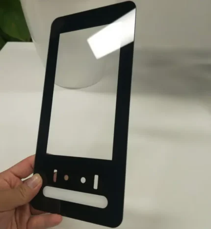
CNC processings:Edge grinding and chamfering, slotting, hole drilling.
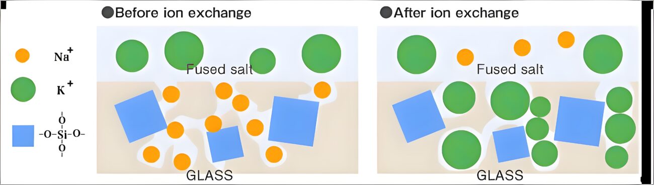
Tempering: Chemically strengthening for thickness under 3.0mm and thermally tempering for 3.0mm thickness above.
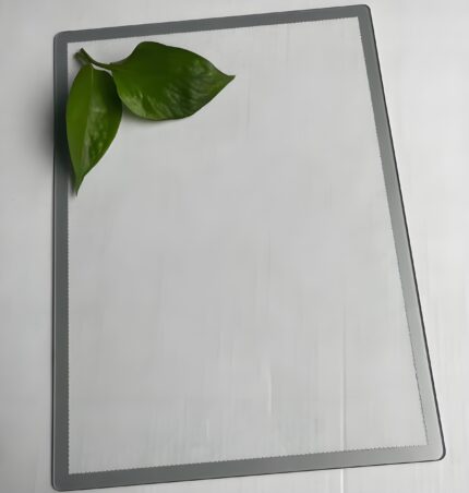
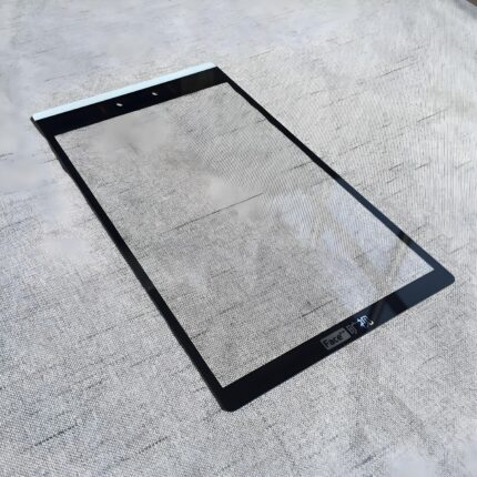
Silk screen print: For thin thickness cover glass option, we use resin ink for print and for thermal tempering we use 3.0mm thickness above.
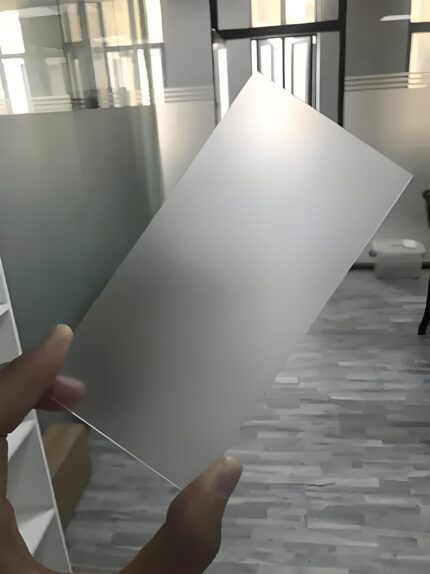
AR means anti reflection by electroplating base on different spectral bands on electronic glass lens, single side increase 3-4% light transittance and double sides up to 99% at most.
AF with 2 kinds of methods including electroplating(costly but more durable) and spray(cheaper but less durable), it can also protect the AR coating from easy peel off.
Bonding: Mainly focus on 3M tapes including adhesive transfer tape, VHB tape and OCA tapes.
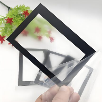
Lamination: Foil to protect from dirt and explosion proof sheet for better anti scatter.
The explaination of chemical strengthened principle
Electronic Glass Materials
Electronic cover glass can be manufactured using different glass substrates depending on the required strength, optical performance, thickness and budget. Common options include soda-lime glass, aluminosilicate glass, Gorilla Glass and other specialty glass substrates.
Electronic Glass Manufacturing Process
Customer Drawing / Sample
↓
Glass Material Selection
↓
Cutting
↓
CNC Machining & Edge Processing
↓
Chemical Strengthening / Thermal Tempering
↓
Silk Screen Printing
↓
AR / AG / AF Coating
↓
Cleaning & Inspection
↓
Packaging & Shipment
Electronic Glass Applications

Display Cover Glass
For LCD, TFT and other electronic displays.
Touchscreen Glass
For touch panels, HMI interfaces and interactive displays.
Consumer Electronics
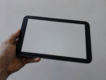
For tablets, POS terminals, smart devices and household electronics.
Industrial Control Panels
For control interfaces, instruments and industrial displays.
Automotive Displays
For vehicle infotainment, instrument clusters and control interfaces.
Medical Devices
For medical monitors, diagnostic equipment and electronic instruments.
Specification For Electronic Glass
| Specification | Options |
|---|---|
| Glass Material | Soda-Lime, Aluminosilicate, Gorilla Glass, Panda Glass |
| Thickness | 0.3–10 mm+ |
| Shape | Round, Square, Rectangle, Custom Shape |
| Size | Customized |
| Edge Processing | Grinding, Polishing, Chamfering, Beveling |
| Strengthening | Chemical Strengthening, Thermal Tempering |
| Printing | Silk Screen Printing |
| Coatings | AR, AG, AF |
| Bonding | 3M Tape, OCA, VHB |
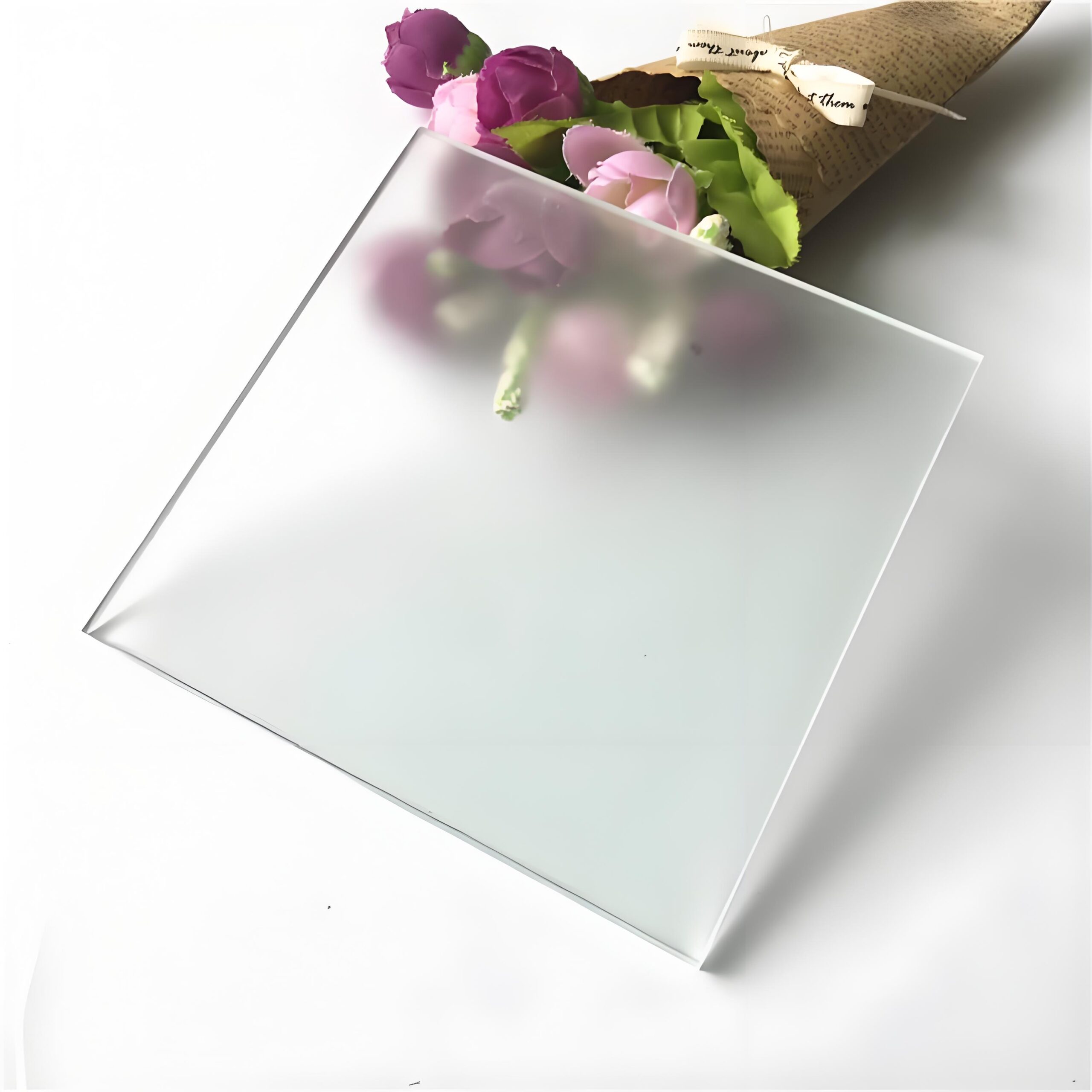
| Surface | Clear, Anti-Glare, Anti-Reflective |
| Application | Displays, Touchscreens, Control Panels, Consumer Electronics |
FAQ
What is electronic glass?
Electronic cover glass is precision-processed glass used in electronic devices, displays, touchscreens, control panels and other applications requiring optical clarity, durability and dimensional accuracy.
What materials can be used for electronic glass?
Common materials include soda-lime glass, aluminosilicate glass, Gorilla Glass and other specialty glass substrates. Material selection depends on the required strength, optical performance, thickness and budget.
What thickness of electronic glass can you manufacture?
We support customized thicknesses based on the application and glass material. Thin electronic cover glass can be chemically strengthened, while thicker glass can be processed with thermal tempering when required.
Can electronic glass be customized in different shapes?
Yes. Electronic glass can be customized according to drawings, samples or specifications. CNC machining can also be used for holes, slots, notches and special contours.
Can electronic glass have AR, AG or AF coatings?
Yes. AR, AG and AF coatings can be applied according to the required optical and surface performance.
Can you provide printed electronic glass?
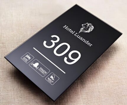
Yes. Silk screen printing can be customized for logos, borders, icons, patterns and other decorative requirements.
Request a Custom Electronic Glass Quote
Send us your glass dimensions, thickness, material, quantity and drawings or samples. Our team will review your requirements and recommend a suitable electronic cover glass solution.